About leadlap Semiconductor
Global Leading Solution Provider of Semiconductor Advance Packaging
Jiangsu Leadlap Semiconductor Technology Co., Ltd. as a core subsidiary of Wuxi Lead Intelligent Equipment Co., Ltd. (LEAD), Dedicated to the research, production, and sales of cutting, grinding, and polishing equipment for semiconductors and related consumables. Our primary focus encompasses advanced packaging laser solutions, thinning machines, CMP equipment, polishing pads, thinning grinding wheels, and other precision processing tools for semiconductors along with their corresponding consumables. We provide high-end semiconductor equipment and services to clients worldwide.


Corporate Video
14000
+
Floor space
200
+
Number of employees
70
+
Intellectual property
Breaking down technological barriers and replacing imports with domestic production
The company to “break the technical barriers, domestic alternative to imports” for the mission, gathering excellent R & D talent at home, the core team from the world's leading semiconductor equipment companies with decades of experience in thinning and polishing, laser equipment research and development and manufacturing.
The company through the flat management mode, professional, efficient and high-quality for the semiconductor industry, high-end customers continue to provide more satisfactory products and services, while integrating and perfecting the global industrial chain, to promote China's semiconductor industry to achieve better and faster forward development of the core technology independently, and gradually become a global semiconductor equipment supplier leading enterprises.


70
+
termHonor

2024
Company culture

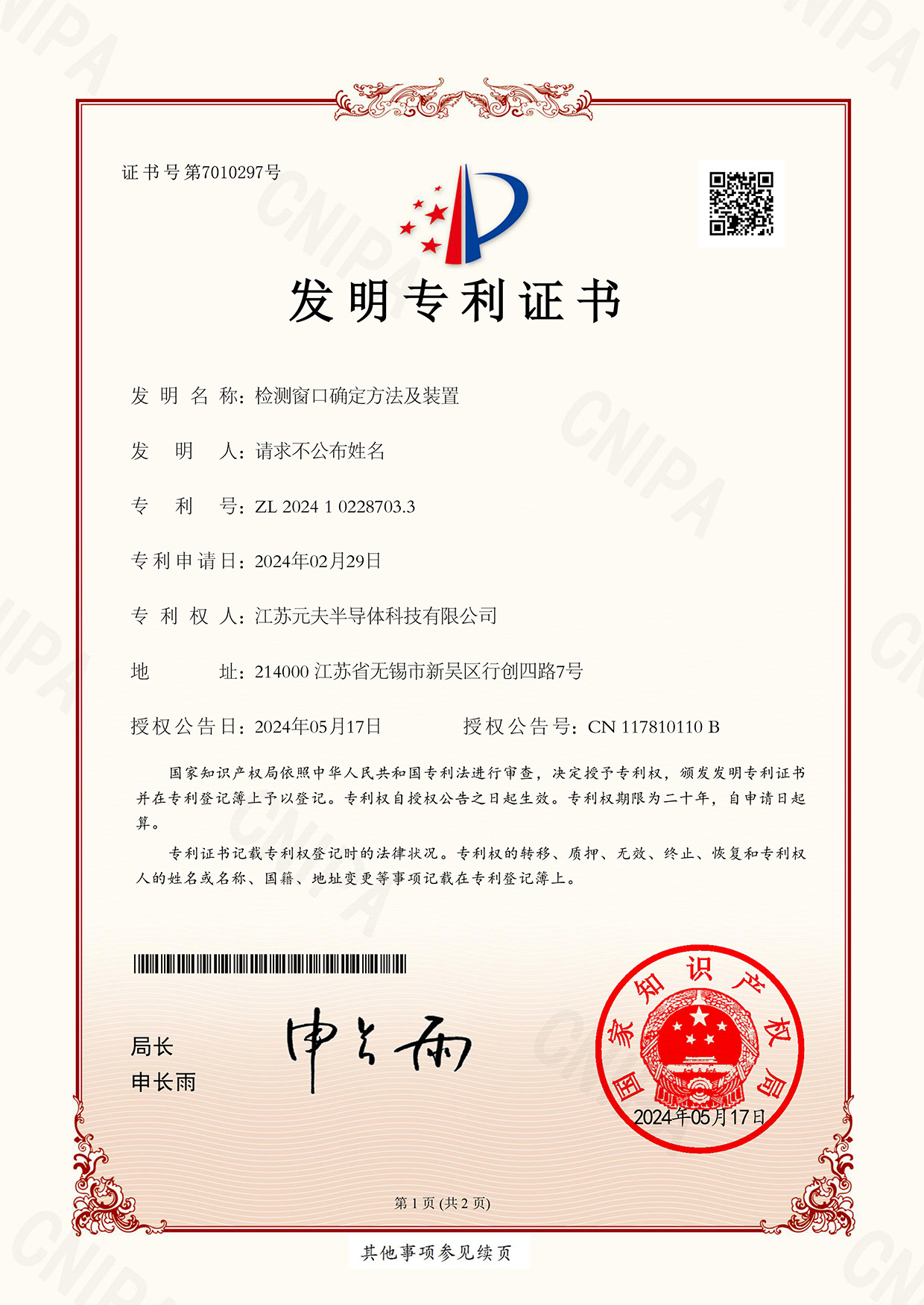
Detection window determination method and device
A laser-induced cutting method and device
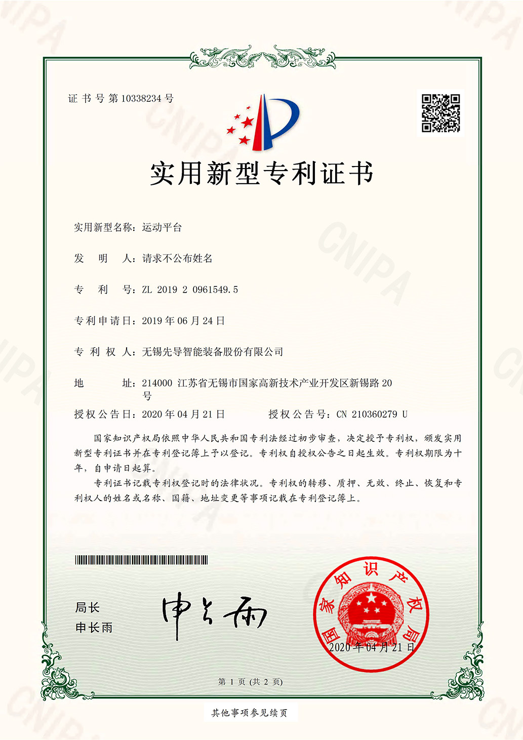
Exercise platforms
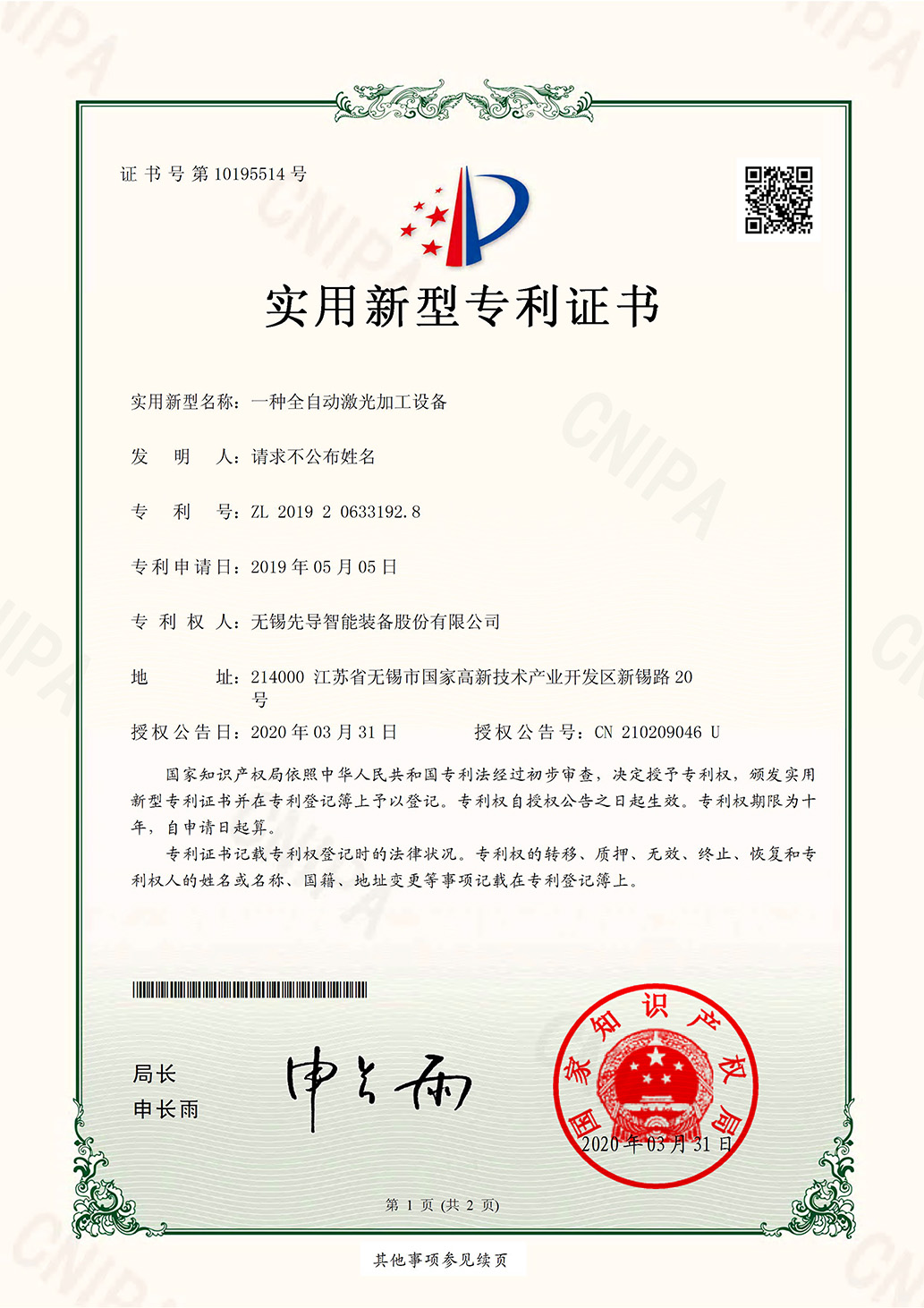
A fully automatic laser processing equipment
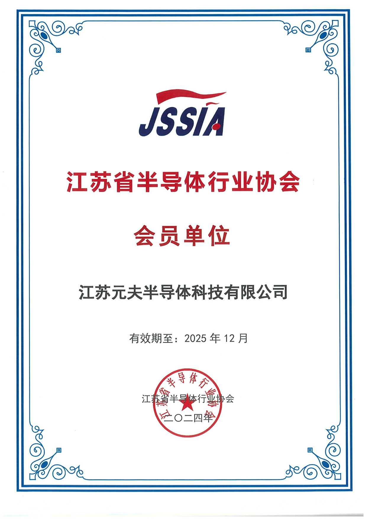
Jiangsu Semiconductor Association Member Certificate
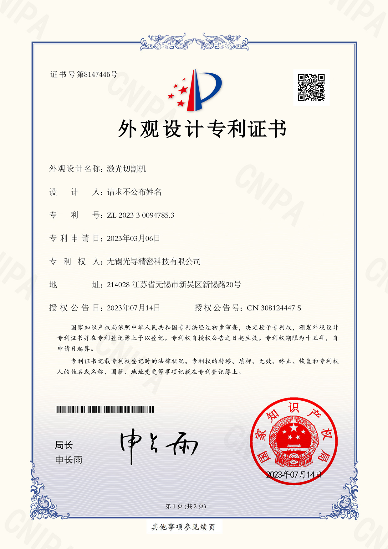
laser cutting machine

